- 您现在的位置:买卖IC网 > Sheet目录483 > NDF08N60ZH (ON Semiconductor)MOSFET N-CH 600V 7.5A TO-220FP
�� �
�
�NDF08N60Z�
�N-Channel� Power� MOSFET�
�600� V,� 0.95� W�
�Features�
�?� Low� ON� Resistance�
�?� Low� Gate� Charge�
�?� ESD� Diode� ?� Protected� Gate�
�?� 100%� Avalanche� Tested�
�?� These� Devices� are� Pb� ?� Free,� Halogen� Free/BFR� Free� and� are� RoHS�
�Compliant�
�ABSOLUTE MAXIMUM RATINGS� (T� C� =� 25� °� C� unless� otherwise� noted)�
�V� DSS�
�600� V�
�http://onsemi.com�
�R� DS(ON)� (MAX)� @� 3.5� A�
�0.95� W�
�Rating�
�Drain� ?� to� ?� Source� Voltage�
�Continuous� Drain� Current� R� q� JC� (Note� 1)�
�Continuous� Drain� Current� R� q� JC�
�T� A� =� 100� °� C� (Note� 1)�
�Pulsed� Drain� Current,�
�V� GS� @� 10� V�
�Symbol�
�V� DSS�
�I� D�
�I� D�
�I� DM�
�NDF08N60Z�
�600�
�8.4�
�5.3�
�30�
�Unit�
�V�
�A�
�A�
�A�
�G� (1)�
�N� ?� Channel�
�D� (2)�
�Power� Dissipation�
�Gate� ?� to� ?� Source� Voltage�
�Single� Pulse� Avalanche� Energy,�
�I� D� =� 7.5� A�
�P� D�
�V� GS�
�E� AS�
�36�
�±� 30�
�235�
�W�
�V�
�mJ�
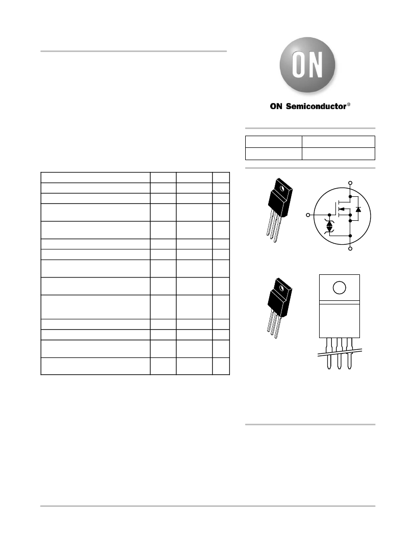
�NDF08N60ZG�
�TO� ?� 220FP�
�CASE� 221D�
�MARKING�
�DIAGRAM�
�S� (3)�
�ESD� (HBM)�
�(JESD� 22� ?� A114)�
�V� esd�
�4000�
�V�
�RMS� Isolation� Voltage�
�(t� =� 0.3� sec.,� R.H.� ≤� 30%,�
�T� A� =� 25� °� C)� (Figure� 14)�
�Peak� Diode� Recovery� (Note� 2)�
�Continuous� Source� Current� (Body� Diode)�
�V� ISO�
�dv/dt�
�I� S�
�4500�
�4.5�
�7.5�
�V�
�V/ns�
�A�
�NDF08N60ZG�
�or�
�NDF08N60ZH�
�AYWW�
�Maximum� Temperature� for� Soldering�
�Leads�
�T� L�
�260�
�°� C�
�NDF08N60ZH�
�TO� ?� 220FP�
�Gate�
�Source�
�Operating� Junction� and� T� J� ,� T� stg� ?� 55� to� 150� °� C�
�Storage� Temperature� Range�
�Stresses� exceeding� Maximum� Ratings� may� damage� the� device.� Maximum�
�Ratings� are� stress� ratings� only.� Functional� operation� above� the� Recommended�
�Operating� Conditions� is� not� implied.� Extended� exposure� to� stresses� above� the�
�Recommended� Operating� Conditions� may� affect� device� reliability.�
�CASE� 221AH�
�A� =� Location� Code�
�Y� =� Year�
�WW� =� Work� Week�
�Drain�
�1.� Limited� by� maximum� junction� temperature�
�2.� I� D� v� 7.5� A,� di/dt� ≤� 200� A/� m� s,� V� DD� ≤� BV� DSS� ,� T� J� ≤� 150� °� C.�
�G,� H�
�=� Pb� ?� Free,� Halogen� ?� Free� Package�
�ORDERING� INFORMATION�
�See� detailed� ordering� and� shipping� information� in� the� package�
�dimensions� section� on� page� 5� of� this� data� sheet.�
�?� Semiconductor� Components� Industries,� LLC,� 2013�
�July,� 2013� ?� Rev.� 3�
�1�
�Publication� Order� Number:�
�NDF08N60Z/D�
�发布紧急采购,3分钟左右您将得到回复。
相关PDF资料
NDF10N62ZG
MOSFET N-CH 620V .75OHM TO220FP
NDF11N50ZG
MOSFET N-CH 500V 12A TO-220FP
NDF11N50ZH
MOSFET N CH 500V 12A TO220FP
NDFEB 6X10MM
MAGNET PERM NDFEB 6.0X10.0MM
NDP6020P
MOSFET P-CH 20V 24A TO-220
NDP6030PL
MOSFET P-CH 30V 30A TO-220
NDP6060L
MOSFET N-CH 60V 48A TO-220AB
NDS0605
MOSFET P-CH 60V 180MA SOT-23
相关代理商/技术参数
NDF10N60Z
制造商:ONSEMI 制造商全称:ON Semiconductor 功能描述:N-Channel Power MOSFET 0.65 ?, 600 Volts
NDF10N60ZG
功能描述:MOSFET NFET T0220FP 600V 10A .65 RoHS:否 制造商:STMicroelectronics 晶体管极性:N-Channel 汲极/源极击穿电压:650 V 闸/源击穿电压:25 V 漏极连续电流:130 A 电阻汲极/源极 RDS(导通):0.014 Ohms 配置:Single 最大工作温度: 安装风格:Through Hole 封装 / 箱体:Max247 封装:Tube
NDF10N60ZH
功能描述:MOSFET NFET 600V 10A RoHS:否 制造商:STMicroelectronics 晶体管极性:N-Channel 汲极/源极击穿电压:650 V 闸/源击穿电压:25 V 漏极连续电流:130 A 电阻汲极/源极 RDS(导通):0.014 Ohms 配置:Single 最大工作温度: 安装风格:Through Hole 封装 / 箱体:Max247 封装:Tube
NDF10N62Z
制造商:ONSEMI 制造商全称:ON Semiconductor 功能描述:N-Channel Power MOSFET 620 V, 0.65 ?
NDF10N62ZG
功能描述:MOSFET Single N-Ch 620V 5.7A, 10A RoHS:否 制造商:STMicroelectronics 晶体管极性:N-Channel 汲极/源极击穿电压:650 V 闸/源击穿电压:25 V 漏极连续电流:130 A 电阻汲极/源极 RDS(导通):0.014 Ohms 配置:Single 最大工作温度: 安装风格:Through Hole 封装 / 箱体:Max247 封装:Tube
NDF11N50Z
制造商:ONSEMI 制造商全称:ON Semiconductor 功能描述:N-Channel Power MOSFET 500 V, 0.52
NDF11N50ZG
功能描述:MOSFET 500V 0.52 OHM TO- 220FP RoHS:否 制造商:STMicroelectronics 晶体管极性:N-Channel 汲极/源极击穿电压:650 V 闸/源击穿电压:25 V 漏极连续电流:130 A 电阻汲极/源极 RDS(导通):0.014 Ohms 配置:Single 最大工作温度: 安装风格:Through Hole 封装 / 箱体:Max247 封装:Tube
NDF11N50ZH
功能描述:MOSFET NFET 500V 10.5A RoHS:否 制造商:STMicroelectronics 晶体管极性:N-Channel 汲极/源极击穿电压:650 V 闸/源击穿电压:25 V 漏极连续电流:130 A 电阻汲极/源极 RDS(导通):0.014 Ohms 配置:Single 最大工作温度: 安装风格:Through Hole 封装 / 箱体:Max247 封装:Tube